A new chapter for advanced chip research and economic growth begins in New York
Husneara Choudhury
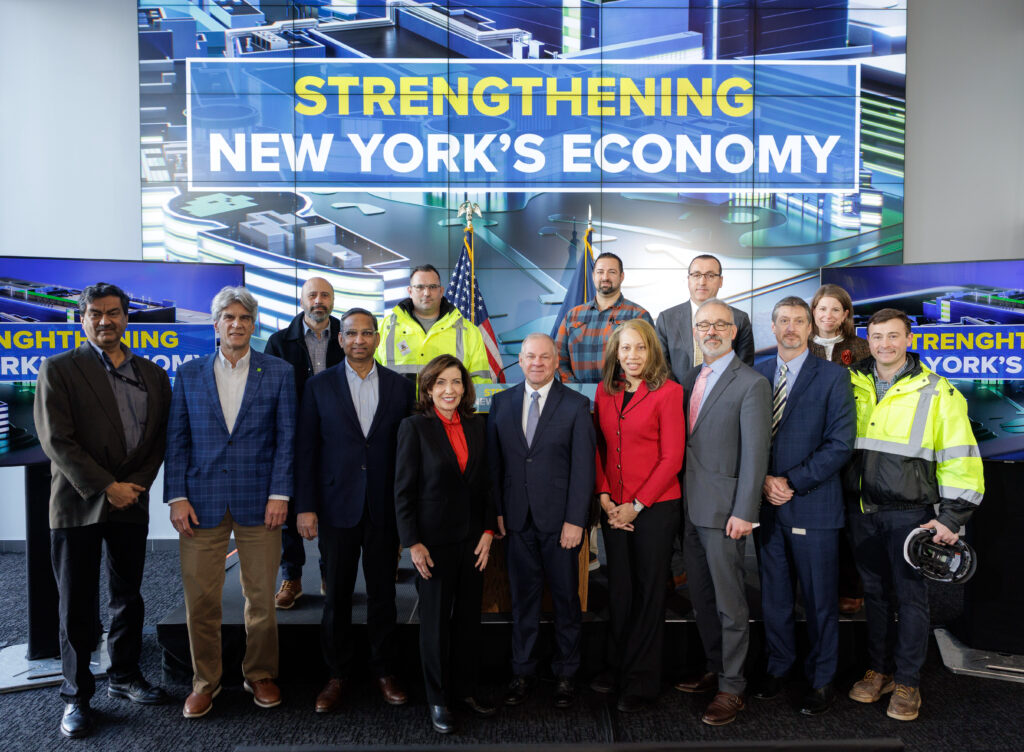
New York: Governor Kathy Hochul today celebrated the “topping out” milestone of the $1 billion NanoFab Reflection project under NY CREATES. This milestone marks the installation of the building’s final steel beam, signaling that the facility is structurally complete and ready for next-generation semiconductor research.
A hub for future chip research
NanoFab Reflection will be North America’s first public High NA EUV lithography facility. Of the 310,000 square feet of research space, approximately 50,000 square feet will be dedicated to state-of-the-art cleanrooms. The facility will house world-class lithography equipment capable of producing faster, more powerful, and energy-efficient semiconductor chips.
Economic and social impact
• Hundreds of new high-tech permanent jobs will be created.
• The project is expected to generate over $9 billion in economic activity, boosting New York’s economy.
• It will foster opportunities for research, industry partnerships, and educational initiatives.
Commitment from state leadership
Governor Hochul said:
“This investment will position New York as a global technology leader — creating jobs, building thriving communities, and driving an innovation-based economy.”
NY CREATES President Dave Anderson added:
“NanoFab Reflection is more than a building — it will help New York lead the way in the future of chip research.”
Background and significance
• The CHIPS and Science Act has renewed national focus on semiconductor production and research.
• The Albany NanoTech Complex is already a leading center for domestic and global chip innovation, and the topping out of NanoFab Reflection marks a new chapter.
• Experts say this investment will strengthen New York’s position in the global semiconductor industry.
